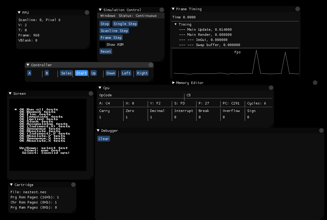
Some of the UI for the Hydra NES emulator, using ImGUI.
Writing an emulator is an incredibly fun learning experience.
It is an exquisite exercise in reverse-engineering from both documentation and code.
In this post I want to share some tips on how and where to start based on my experience on the NES emulator I am writing.
Information
The gathering of information is the most important (and hard!) process that will live through all the writing process.
Luckily for us there are many websites to help in this:
https://wiki.nesdev.com/w/index.php/NES_reference_guide
http://obelisk.me.uk/6502/reference.html
http://www.oxyron.de/html/opcodes02.html
It is paramount to create a list of websites and resources (maybe through some notes, like in Evernote or such) about different topics regarding the hardware to be emulated.
Having a central hub is powerful and counteract the sparseness of the different informations (some in txt files, different websites, forum blogposts, …).
I can’t stress enough how important it is.
The amazing NesDev Wiki is the hub you need. Almost every possible information is there.
Architecture
Next step is to understand the architecture. Write diagrams, take notes, search for the relationships of the component. What does every hardware component do ? What can that specific hardware piece access to ?
As you will see, writing the emulator is an iterative process of improving each component until you have something that works very well, and then refine for an infinite amount of time. On a very basic level, there should be a CPU, some form of GPU (PPU, Picture Processing Unit), some audio chip, some input peripheral and cartridge/disc/rom.
NES architecture
The NES is a beautiful machine equipped with the following:
CPU : Ricoh RP2A03 (NTSC) / RP2A07 (PAL)
8 bit processor that contains both CPU and APU (audio) hardware. The addresses are 16 bit, but the data is 8. It contains only specific registers: 2 indices, accumulator, stack pointer, program counter and status.
PPU : Ricoh RP2C02 (NTSC) / RP2C07 (PAL)
This is what today would be called GPU. It outputs to a 256x240 pixels buffer, it has 2kib or RAM, 32 bytes for palette RAM and 288 bytes for sprite RAM. The PPU is tile based and it takes 8 PPU cycles to load a line of a background tile. Sprites are sent through DMA and background is filled during Vertical Blank state normally. A frame lasts more scanline that the one visible, so that the game can upload data to the PPU when not rendering.
APU : Ricoh RP2A03 (NTSC) / RP2A07 (PAL) (Contained in the CPU itself.)
The sound is analogic and it comes from 5 different channels: 2 pulse, 1 triangle, 1 noise and 1 DMC. All the channels aside from the DMC create signals that are combined to output the sounds and music. The DMC loads samples using the DMA.
Cartridge/Mappers :
This is a very unique topic strict to the NES as far as I know. Cartridges had unique hardware and they were used to swap banks of memory in realtime to access different parts of the cartridge. There are hundred of mappers that have unique behaviours! The biggest gist of the mappers is how they switch banks: by WRITING to the address where the execution code is it triggers the bank-switching logic. There can be internal batteries and working RAMs too, but they are very rare.
Memory mapped I/O
The different hardware access using ‘memory mapped I/O’, that is a way of saying that when you read or write to a specific address it could be memory or it could be an hardware-component.
Examples: reading from address 0x4016 gives you the gamepad status, while reading from 0x1000 reads from the CPU ram.
Having clear these accesses will help in understanding even better the machine.
Both CPU and PPU have different memory maps. Let’s see them, it will help in understanding the internal of the NES better.
CPU Memory Map
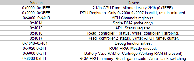
The CPU can access basically every hardware component in the NES. PPU, APU, gamepads, both read and write.
It reads the ROM part of a cartridge (called PRG) and executes its instructions. Through PPU registers it can instruct the PPU to read graphical informations from the CHR part of the cartridge. It can upload sprites on the PPU Sprite Memory through DMA, upload data to the APU, or manage its internal RAM.
From the source code, this is a working example of CPU Reading method:
uint8 Nes::MemoryController::CpuRead( uint16 address ) {

    if ( address < 0x2000 ) {
        return cpu->ram[address & 0x7FF];
    }
    else if ( address < 0x4000 ) {
        return ppu->CpuRead( address );
    }
    else if ( address < 0x4014 ) {
        return apu->CpuRead( address );
    }
    else if ( address >= 0x4018 ) {
        return mapper->PrgRead( address );
    }

    switch ( address ) {
        case 0x4015: {
            return apu->ReadStatus();
            break;
        }

        case 0x4016: {
            return controllers->ReadState();
            break;
        }

        case 0x4017: {
            return 0x40;
            break;
        }
    }

    return 0;
}
And CPU Write:
void Nes::MemoryController::CpuWrite( uint16 address, uint8 data ) {

    if ( address < 0x2000 ) {
        cpu->ram[address & 0x7FF] = data;
    }
    else if ( address < 0x4000 ) {
        ppu->CpuWrite( address, data );
        return;
    }
    else if ( address < 0x4014 ) {
        return apu->CpuWrite( address, data );
    }
    else if ( address >= 0x4018 ) {
        mapper->PrgWrite( address, data );
        return;
    }

    switch ( address ) {
        // Sprite DMA
        case 0x4014: {
            cpu->ExecuteSpriteDMA( data );
            return;
            break;
        }

        case 0x4015:
        case 0x4017: {
            apu->CpuWrite( address, data );
            return;
            break;
        }

        case 0x4016: {
            controllers->WriteState( data );
            return;
            break;
        }
    }
}
The pattern is always the same: check the address of the instruction and choose which hardware component to interact with.
Hopefully its clear that based on the address different components can be accessed. Let’s have a look at the PPU too.
PPU Memory Map
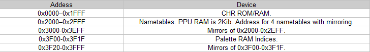
Similar to the CPU, reading and writing on the PPU access different components, even though they are far less. The PPU either accesses its 2 rams (palette and nametable, normally from the CPU) or reads the CHR (that is the graphical data stored in the cartridge) memory.
Reading:
uint8 Nes::MemoryController::PpuRead( uint16 address ) {

    address &= 0X3FFF;

    if ( address <= 0x1FFF ) {
        return mapper->ChrRead( address );
    }
    else if ( address <= 0x3EFF ) {
        return ppu->nametableRam[NameTableMirroring( address, mapper->mirroring )];
    }
    else if ( address <= 0x3FFF ) {
        // Palette mirroring is handled in the write code.
        return ppu->paletteRam[address & 0x1F] & ((ppu->mask & Nes::Ppu::MaskFlag_GreyScale ? 0x30 : 0xFF));
    }
    return 0;
}
On the writing side, there the code shows the intricancy of emulation. When writing to the paletter ram, there is a mirroring mechanism happening in the hardware that is emulated with a lookup table. Something to look out to: writing to CHR is 99% of the time useless, unless there is an additional RAM in the cartdige.
void Nes::MemoryController::PpuWrite( uint16 address, uint8 data ) {

    address &= 0X3FFF;

    if ( address <= 0x1FFF ) {
        mapper->ChrWrite( address, data );
        return;
    }
    else if ( address <= 0x3EFF ) {
        ppu->nametableRam[NameTableMirroring( address, mapper->mirroring )] = data;
        return;
    }
    else if ( address <= 0x3FFF ) {

        static uint8 const palette_write_mirror[0x20] = {
            0x10, 0x01, 0x02, 0x03, 0x14, 0x05, 0x06, 0x07,
            0x18, 0x09, 0x0A, 0x0B, 0x1C, 0x0D, 0x0E, 0x0F,
            0x00, 0x11, 0x12, 0x13, 0x04, 0x15, 0x16, 0x17,
            0x08, 0x19, 0x1A, 0x1B, 0x0C, 0x1D, 0x1E, 0x1F };

        ppu->paletteRam[palette_write_mirror[address & 0x1F]] = data;
        return;
    }
}
Takeaways
I created the memory controller as the main dispatcher of data between hardware components, to separate the duties better. We can see the following relationships based on that:
- CPU can access PPU, APU, controllers and cartridge (PRG)
- PPU can access screen, its own rams and cartridge (CHR)
- memory controller is the hub that connects everything
I am not sure this is the best emulator architecture, but that is what I figured out.
Test roms
A fundamental approach to create a robust emulator is to have some tests to rely on. Sadly it is not common for all hardware, but again the NES provide plenty of roms that tests almost every aspect of your emulator! It quickly becomes a test-driven development.
Find roms, read the source code and try to understand what they are doing and why.
Coding start
If you are writing your first emulator, I suggest to focus mostly on the emulation part.
What do I mean by that ? Avoid trying too many things at once! Focus your energies towards the emulation. Use libraries that are reliable and simple and that you know. GLFW, SDL2, etc are your friends here. You want to eliminate most unknowns unknowns before hand. Of course, if you are brave enough, you can also write an emulator in a new language.
But for me, I preferred to concentrate on the emulation side first, in C++, using my core library, especially knowing that I could dedicate some night-time here and there, No surprises (not really true, still some happened!).
I will possibly port the emulator to use SDL if needed, but right now the emulation code is the most important.
This is the mantra that helped me concentrate only on the emulation code. Again, writing-wise I am not happy about the code quality. But what I am learning from different perspectives is invaluable!
NES coding start
The quintessential basic steps to start a NES emulator coding are:
- Write CPU basics (fetch/decode/execute loop, registers)
- Basic memory bus (read/write to/from memory and registers)
- Load a rom and start executing instruction step by step.
It is already a lot, and it will require to read multiple times the different wiki pages and forum posts.
For a typical console, the main loop (simplified) can be something like this:
void CpuTick() {
    uint8_t opcode = Read(program_counter++);
    uint8_t operand = FetchOperand(opcode);
    ExecuteOpcode(opcode, operand);
}

void ExecuteFrame() {
    uint32_t cycles_per_frame = …

    while (cycles_per_frame — ) {
        CpuTick();
    }
}
To jumpstart your NES emulator you can use the majestic rom nestest.nes and its log file: it gives you a test of all instructions of the CPU and prints the status of the CPU after each one.
Also it does not require any PPU rendering: compare the status of your CPU with the text file line by line and its done!
You can see some ugly but useful code in MainState::ExecuteCpuTest in my emulator for an idea.
A line from the nestest.log file looks like this:
// C000 4C F5 C5 JMP $C5F5 A:00 X:00 Y:00 P:24 SP:FD PPU: 0, 0 CYC:7
it gives you the ProgramCounter (C000), byte code (1, 2 or 3 bytes depending on the instructions), human-readable-instruction (JMP) , the CPU register contents (A, X, Y, P, SP) and the theorethical PPU scanline, pixel and clock cycle.
There are two interesting points:
- The ProgramCounter before execution should be set to C000 for this rom only and only when logging.
- The CPU cycles STARTS at 7. In a power-up/reset method there is some work done BEFORE executing any code. This is needed only if you want to have a precise cycle-to-cycle comparison.
You can create a simple test method like this:
void TestEmulatorCPU() {
    Reset();

    while(true) {
        CpuTick();
        CompareCpuStatusWithLog();
    }
}
and catch the problems in your CPU instructions implementation!
Conclusion
This is a little help in understanding how to start with an emulator.
It is a beautiful journey, but it is full of trial and errors.
I am myself far from over with my emulator, and also far from being happy on HOW I write the emulator itself.
There are emulators of much more complex machines out there (almost every machine you can imagine!) and it blows my mind to know there are people that can emulate such complex hardware.
The ideal situation would be to being able of not being lost in visual emulation of the circuitry, but for now that is out of my league.
I am thinking of creating some a series of videos and code associated starting from scratch, if anyone is interested. Please leave a comment/feedback on the article, the source code, anything!
I hope it will help.